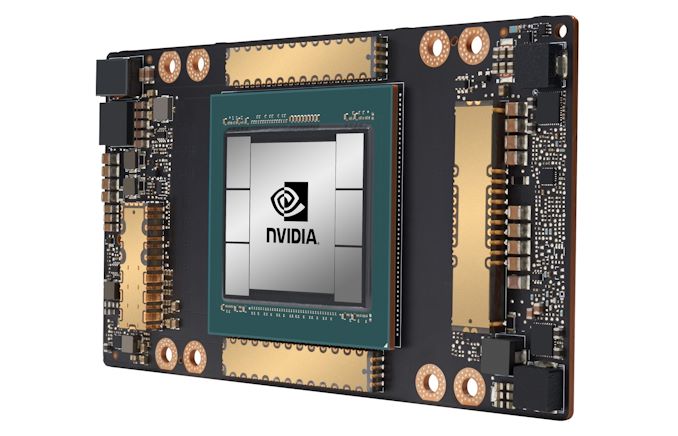
Tesla A100 GPU series:

Image courtesy: Nvidia
The latest Nvidia successor to Volta series of GPUs from is out. It's the Ampere series. With over 54 Billion transistors in the latest Tesla A100 GPU, it is seemingly the most powerful GPU on the planet right now in terms of vRAM, Cuda Cores and the effective compute capability.
The reason Nvidia's been able to fit in so many transistors and CUDA cores in their Ampere GPUs is because they are the world's first 7nm fabricated chipsets.
NVIDIA Ampere design comes along with third-generation Tensor cores called TF32 designed specifically for AI compute applications. The latest Tensor cores support more flops on FP64 computing, which is a much needed precision performance for High performance computing industry. Specially the Simulation domain.
GPU Memory:
To be able to perform massive computational throughput, the NVIDIA A100 GPU comes with 40 GB of fast-speed HBM2 memory with a top of the class 1.6 TB/sec of memory bandwidth – a 73% increase compared to Tesla V100's 900 GB/sec.
In addition, the A100 GPU has significantly more on-chip memory including a 40 MB Level 2 (L2) cache—nearly 7x larger than V100—to maximize compute performance.
But how does it perform in practice against the predecessor GPUs like Nvidia Tesla V100?
Benchmarks:
The real GPU benchmarks for Nvidia Tesla A100 cards are here and they are turning out to be as fast as the upgrade in their transistor count compared to Tesla V100s.
Below is a quick comparsion of the performance results between Tesla A100 and Tesla V100 on Resnet 50 model with half precision (FP16) and single precision (FP32) performance numbers:
Benchmark type: Resnet 50 with FP16
| # | Batch Size | Nvidia Tesla A100 | Nvidia Tesla V100 |
|---|---|---|---|
| 1 | 128 | 1714 Images/sec | 963 Images/sec |
| 2 | 256 | 1918 Images/sec | 1006 Images/sec |
Benchmark type: Resnet 50 with FP32
| # | Batch Size | Nvidia Tesla A100 | Nvidia Tesla V100 |
|---|---|---|---|
| 1 | 64 | 733 Images/sec | 367 Images/sec |
| 2 | 128 | 794 Images/sec | 392 Images/sec |
As you can see, the Tesla A100 is almost 2X as fast as a Tesla V100 for the number of images processed per second while training AI neural nets.
The major reason for this increase in the performance value is because of more memory, higher memory bandwidth, more core count and new Ampere architecture streaming multiprocessors.
The Nvidia Ampere architecture-based A100 Tensor Core GPU significantly increases performance, builds upon features introduced in both the Volta and Turing SM architectures, and adds many new capabilities.
Along with the support for sparse matrix manipulation and using the latest Tensor cores, it will even surpass the above benchmarks.
There are a couple more exceptional qualities about Tesla A100 that makes it the best GPU to serve almost any existing computing workload:
Multi-Instance GPU (MIG) partition:
MIG enabled Tesla A100s allows a user to partition the GPU into as many as seven independent GPU instances with all the GPU instances running simultaneously and each instance having its own memory, cache and streaming multiprocessors.
Multi-tenancy becomes a piece of cake with MIG virtualization on Tesla A100 GPUs.
PCIe Generation 4:
The Tesla A100 GPUs support PCI Express Gen 4 which provides 2x bandiwidth of 31 GB/sec compared to PCIe 3.0 which had 15 GB/sec for 16x lanes. A100 also supports SR-IOV i.e. single root input/output virtualization, which allows sharing and virtualizing a single PCIe connection for multiple processes or VMs.
All in all, the Tesla A100 seems to be a really powerful GPU with a beafed up vRAM and memory bandwidth to cater to the much more compute intensive workloads in AI and HPC industry.


